SiC Crystal Crucibles - OEM Graphite Machining Manufacturer Logo
SiC Crystal Crucibles
Start inquiry
SiC Crystal Crucibles - OEM Graphite Machining Manufacturer Logo
SiC Crystal Crucibles
Consult Engineering via WhatsApp
SiC Crystal Crucibles - OEM Graphite Machining Manufacturer Logo
SiC Crystal Crucibles

China-based custom graphite manufacturer supporting precision machining, RFQ-defined ash targets, and export delivery planning.

Inquiry Email

[email protected]

Email app

Attach DWG, STEP, or PDF drawings and include purity, tolerance, quantity forecast, and delivery country.

Instant Chat

+8618857971991

Chat on WhatsApp

Use WhatsApp for quick engineering clarification before a formal quote.

Factory Addr:Liaoyang, Liaoning, China (Xingde Graphite manufacturing partner)

Email:[email protected]

WhatsApp:+86 18857971991

Products & Consumables
  • SiC Crystal Growth Crucible
  • TaC Coated Crucible
  • High-Purity Graphite Crucible
  • Isostatic Graphite Crucible
  • SiC PVT Crucible
  • Porous Graphite (TaC)
  • Graphite Susceptor
  • MOCVD Wafer Carrier
  • Graphite Heater
  • Graphite Hot Zone
  • PAN Carbon Felt
  • Graphite Felt Insulation
  • Rigid Carbon Felt Board
  • Graphite Crucible Lid & Cover
  • CVD-SiC Coated Susceptor
  • Semiconductor Graphite Machining
Solutions & Applications
  • SiC PVT Crystal Growth
  • SiC Wafer Manufacturing
  • Vacuum Furnace Hot Zone
  • Crystal Growth Laboratory
  • High-Temperature Furnace Consumables
OEM Capabilities
  • High-Temp Purification
  • CVD Coating Service
  • Precision Machining
  • Ash PPM & Impurity Control
  • Drawing-Based Graphite Parts
  • Inspection & Packaging
Resources
  • Insights
  • About Factory
  • Request a Quote
  • Privacy Policy
  • Terms of Service
© 2026 SiC Crystal Crucibles. All Rights Reserved.|Manufacturing support coordinated with Liaoyang Xingde Graphite for high-purity isostatic graphite machining and purification.
← Back to OEM Capabilities

CVD TaC & SiC Coating Service

CVD TaC and CVD-SiC coating support for graphite crucibles, liners, susceptors, wafer carriers, and hot-zone parts requiring stronger chemical isolation or particle control.

Best Fit For:PVT, epitaxy, and semiconductor equipment engineers qualifying coated graphite parts by drawing.
Cvd Coating Service - CVD TaC/SiC Coating Solution

Capability Highlights

  • TaC and CVD-SiC coating route reviewed by process chemistry and temperature
  • Coating surface map, thickness target, and masked zones aligned before production
  • Base graphite grade, purification, cleaning, and thermal-cycle duty reviewed together

Typical Engagement Scope

  • TaC coated graphite crucibles and liners for SiC PVT growth
  • CVD-SiC coated graphite susceptors and wafer carriers for epitaxy
  • Coated graphite hot-zone parts exposed to corrosive or contamination-sensitive environments

Execution Focus

  • Base graphite density, surface preparation, and coating adhesion risk
  • Coating thickness uniformity, coverage around grooves, bores, and threads
  • Cleaning chemistry, ramp rate, handling method, and inspection acceptance criteria

Program Evaluation Matrix

Program MetricTypical RangeProcurement Value
Coating SelectionTaC or CVD-SiC by process chemistryTaC and SiC coatings solve different high-temperature, corrosion, and contamination problems.
Coating ThicknessDefined by RFQ, geometry, and inspection planThickness affects coverage, thermal stress, feature fit, cleaning durability, and cost.
Surface Map CompletenessCoated, uncoated, masked, and mating zones markedA clear surface map prevents exposed graphite, coating on functional fits, and quote ambiguity.

RFQ Preparation Checklist

  1. Part drawing with coated, uncoated, masked, and mating surfaces marked
  2. Base graphite grade, density, ash target, and pre-coating purification need
  3. Coating material, target thickness range, and critical coverage areas
  4. Operating temperature, atmosphere, gases, cleaning method, and cycle length
  5. Inspection criteria, sample quantity, annual forecast, destination, and timeline

Risk and Mitigation

  • Microcracks or delamination: Review base graphite grade, surface preparation, coating thickness, thermal cycling, and ramp assumptions before sample approval.
  • Coating on mating or tolerance-critical faces: Mark masked surfaces, contact faces, bores, threads, and inspection dimensions directly on the drawing.
  • Wrong coating chemistry: Confirm process gases, cleaning chemistry, temperature window, and contamination limits before selecting TaC or CVD-SiC.

Related Products

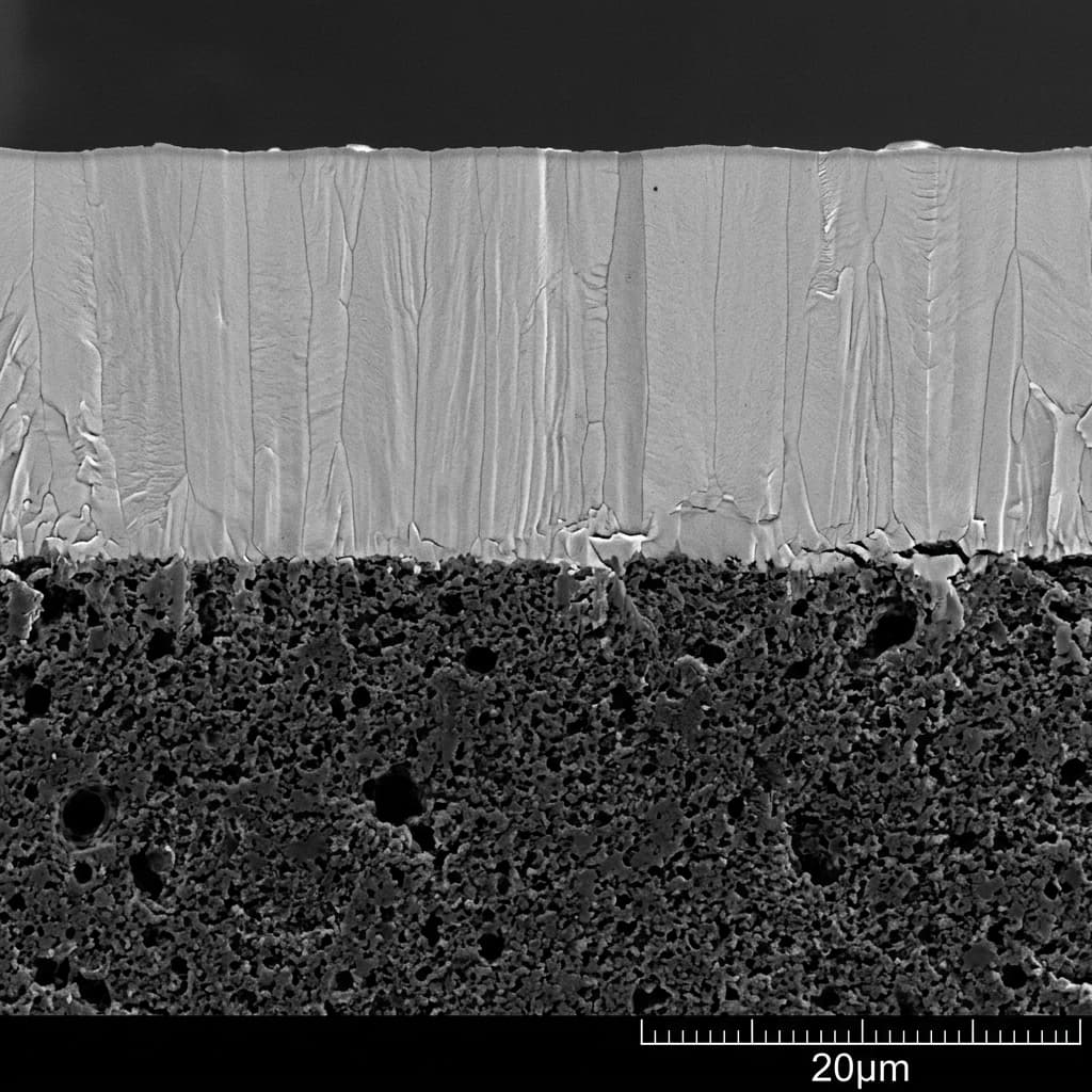
SEM cross-section micrograph of TaC CVD coating showing dense columnar microstructure
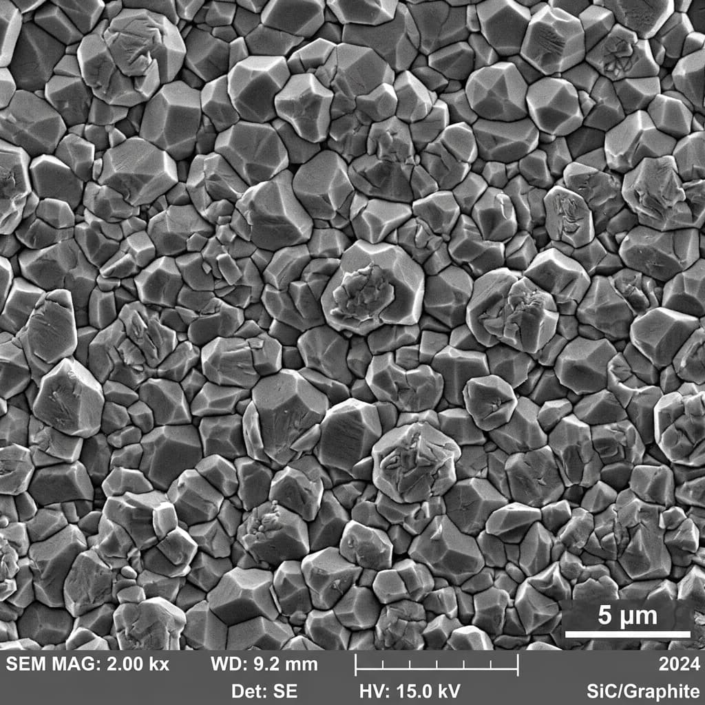
SEM surface morphology of CVD-SiC coating showing pinhole-free polycrystalline structure
Cvd Coating Service - CVD TaC/SiC Coating Solution

Decision fit

Who should evaluate this

PVT, epitaxy, and semiconductor equipment engineers qualifying coated graphite parts by drawing.

Primary proof point

Coating Selection

TaC or CVD-SiC by process chemistry

TaC and SiC coatings solve different high-temperature, corrosion, and contamination problems.

RFQ trigger

Data needed first

  • Part drawing with coated, uncoated, masked, and mating surfaces marked
  • Base graphite grade, density, ash target, and pre-coating purification need
  • Coating material, target thickness range, and critical coverage areas

Selection and Acceptance Logic

Decision GateWhat Buyers Should CheckAcceptance Evidence
Use-case fitTaC coated graphite crucibles and liners for SiC PVT growth; CVD-SiC coated graphite susceptors and wafer carriers for epitaxy; Coated graphite hot-zone parts exposed to corrosive or contamination-sensitive environmentsApplication, furnace duty, and buyer-side validation goal are confirmed before material or process route selection.
Parameter baselineCoating Selection: TaC or CVD-SiC by process chemistry; Coating Thickness: Defined by RFQ, geometry, and inspection plan; Surface Map Completeness: Coated, uncoated, masked, and mating zones markedTarget ranges, report needs, and pass/fail criteria are written into the RFQ or sample approval plan.
Risk closureMicrocracks or delamination: Review base graphite grade, surface preparation, coating thickness, thermal cycling, and ramp assumptions before sample approval.; Coating on mating or tolerance-critical faces: Mark masked surfaces, contact faces, bores, threads, and inspection dimensions directly on the drawing.Drawing notes, inspection scope, cleaning, coating, packaging, and traceability controls are agreed before repeat supply.
RFQ completenessPart drawing with coated, uncoated, masked, and mating surfaces marked; Base graphite grade, density, ash target, and pre-coating purification need; Coating material, target thickness range, and critical coverage areas; Operating temperature, atmosphere, gases, cleaning method, and cycle lengthEngineering can return a quote direction without avoidable loops for drawing, purity, coating, quantity, or delivery gaps.

Factory Execution Path

  1. 1

    Confidential RFQ intake

    Collect CAD, drawings, specifications, target reports, and NDA expectations before engineering review starts.

  2. 2

    DFM and risk review

    Check machinability, material grade, purity path, coating feasibility, tolerance stack-up, and packaging risk.

  3. 3

    Sample and inspection package

    Prepare sample scope with dimensional evidence, material records, cleaning notes, and acceptance criteria.

  4. 4

    Production handoff

    Lock revision control, batch traceability, inspection cadence, export documents, and delivery plan for repeat orders.

Evidence Buyers Can Request

  • Revision-controlled drawing pack and DFM comments before machining approval
  • Material, purification, coating, and inspection records agreed by program stage
  • Dimensional report, photo evidence, and packaging record for sample lots
  • Change-control path for post-sample engineering updates and repeat production

Claim Boundaries

  • DFM comments are preliminary until final drawings, tolerances, material route, and acceptance criteria are approved.
  • Quoted lead time and inspection scope depend on geometry complexity, purification depth, coating scope, and destination documents.
  • NDA, compliance, origin, and certification requests should be declared before quotation so document availability is explicit.

Next Internal Links

Semiconductor graphite machining

See the product-side machining scope for semiconductor graphite components.

Graphite hot zone

Connect OEM execution to complete furnace hot-zone component programs.

Request a quote

Send drawings, purity targets, forecast quantities, destination, and delivery timeline.

TaC Coated Graphite Crucible

Open the related page to continue technical qualification.

CVD-SiC Coated Graphite Susceptor

Open the related page to continue technical qualification.

Inquiry Email

[email protected]

Email app

Attach DWG, STEP, or PDF drawings and include purity, tolerance, quantity forecast, and delivery country.

Instant Chat

+8618857971991

Chat on WhatsApp

Use WhatsApp for quick engineering clarification before a formal quote.

Buyer FAQ

Can you coat porous graphite?

Porous graphite can be reviewed for conformal coating, but porosity, permeability, particle limits, and coating thickness must be aligned before quoting.

Do you need a coating surface map?

Yes. Coated, uncoated, masked, and mating surfaces should be marked to avoid coverage gaps or coating on functional interfaces.

Can coating be applied after purification?

Yes. Many coated graphite programs route through machining, purification, surface preparation, CVD coating, cleaning, inspection, and packaging.