
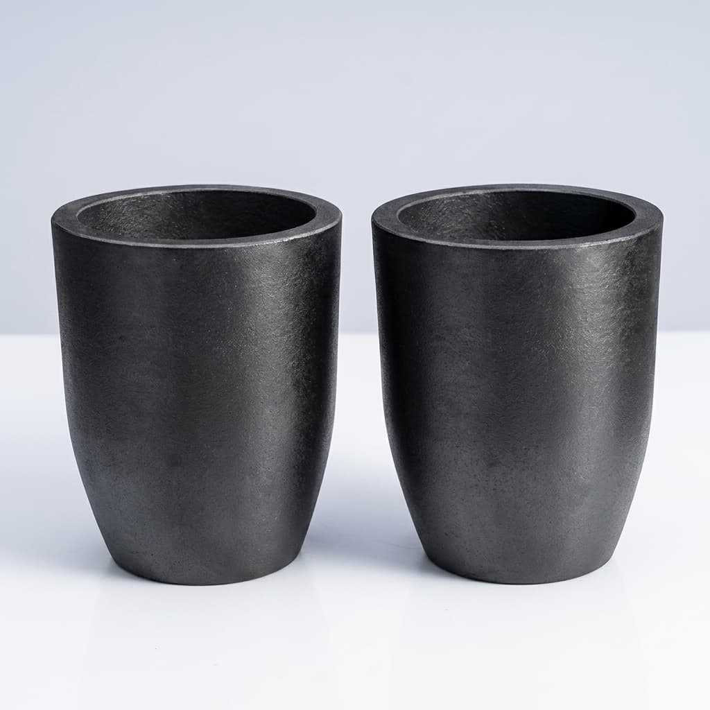
Trace Metal Contamination in SiC PVT Growth: GDMS Benchmarks and Halogen Purification
How halogen purification removes Boron, Vanadium, and Iron from graphite crucibles. A procurement guide to GDMS purity specifications for semi-insulating SiC.
In the Physical Vapor Transport (PVT) process for Silicon Carbide (SiC) crystal growth, the environment operates at extremes. At temperatures exceeding 2,200°C within a vacuum or inert argon atmosphere, the graphite crucible is not merely a passive vessel; it is an active participant in the thermodynamic system.
For engineers and procurement teams targeting semi-insulating (SI) SiC wafers or low-defect n-type substrates, the purity of the graphite hot zone is a critical yield determinant. Even parts-per-million (ppm) levels of metallic impurities in the graphite matrix will volatilize, migrate through the vapor phase, and incorporate into the growing SiC boule. This trace metal contamination disrupts the delicate C/Si ratio, shifts electrical resistivity, and nucleates defects such as micropipes and basal plane dislocations (BPD). For component geometry and RFQ context, compare the SiC crystal growth crucible page alongside your furnace drawing package.
This technical brief details the engineering limits of standard vacuum baking, explains the mechanism of halogen purification, and provides specific Glow Discharge Mass Spectrometry (GDMS) benchmarks for SiC crucible procurement. It applies to graphite hot-zone components for 150mm and 200mm SiC PVT growth as of July 20, 2026; final limits still need validation against each buyer's furnace design, dopant recipe, post-growth SIMS/GDMS data, and wafer electrical map.
1. Applicable Boundaries: Where Halogen Purification is Mandatory
Not all SiC applications require sub-ppm halogen-purified graphite. Understanding the applicable boundaries (适用边界) helps procurement teams avoid over-specifying and over-paying for crucibles. The distinction primarily depends on the final application of the silicon carbide wafers being produced.
Semi-Insulating (SI) SiC for RF Devices: This is the strictest boundary. SI-SiC wafers used for 5G base stations, military radar, and aerospace communication systems rely on deep-level compensation (typically through intentional Vanadium doping) to achieve extremely high electrical resistivities above 10^5 ohm-cm. In these systems, any unintended shallow donors (like Nitrogen) or shallow acceptors (like Boron or Aluminum) can disrupt this delicate charge compensation balance. If Boron escapes from the crucible during growth, the wafer can become slightly conductive, damaging its RF insulating properties. Therefore, halogen purification targeting Boron below 0.1 ppm is strictly mandatory here.
Low-Defect n-type SiC for Power Electronics: Wafers destined for automotive EV traction inverters, solar micro-inverters, and high-voltage grid infrastructure are heavily doped with Nitrogen to achieve very low resistivity below 0.02 ohm-cm. While these n-type wafers are generally less sensitive to trace amounts of Boron than SI-SiC, they are extraordinarily sensitive to transition metals like Iron, Titanium, and Nickel. During growth, transition metal clusters can serve as active nucleation sites for severe crystal defects, specifically micropipes and Basal Plane Dislocations (BPDs). These defects cause catastrophic leakage currents in the final MOSFET devices. Standard vacuum baking is insufficient to remove these heavy metals; halogen purification is highly recommended to maximize wafer yield.
Abrasives, Gemstones, and Structural SiC: For non-electronic applications, such as synthetic moissanite gemstones, industrial abrasives, or structural armor plating, the electronic properties are irrelevant. Standard high-temperature vacuum baked graphite may be adequate when the buyer's acceptance plan is based on mechanical performance rather than electrical purity. Specifying expensive halogen-purified graphite for these applications is often unnecessary capital expenditure.
2. Specification Dimensions: Defining the Crucible
When defining the specification dimensions (规格维度) for a SiC PVT crucible, chemical purity is only one axis. Engineering teams must specify a multi-dimensional matrix to ensure the hot zone performs predictably over a 100+ hour growth cycle. If your procurement scope includes lids, liners, insulation, and spacers, align this article with the broader SiC PVT crystal growth solution checklist before issuing a supplier RFQ:
- Apparent Density: Typically mandated above 1.82 g/cm^3. Higher density reduces the total surface area available for outgassing and significantly improves the mechanical strength of the thin-walled crucible, preventing sagging at 2,300°C.
- Open Porosity: Must be strictly minimized, typically below 10%. High porosity allows aggressive Silicon vapor to easily penetrate the crucible wall. Once inside, it reacts with the carbon to form SiC. This localized conversion leads to premature mechanical failure due to coefficient of thermal expansion (CTE) mismatches between the unreacted graphite and the newly formed SiC.
- Coefficient of Thermal Expansion (CTE): Should be matched as closely as possible to the growing SiC crystal, typically ranging from 4.0 to 4.5 x 10^-6 /K. Mismatched CTE can induce immense stress during the cooling phase, leading to basal plane dislocations or even shattering the boule.
- Thermal Conductivity: Isotropic thermal properties are critical. The crucible acts as the primary thermal susceptor, coupling with the RF induction coils to generate heat. Inconsistent or anisotropic thermal conductivity leads to asymmetric radial temperature gradients inside the growth chamber, causing curved isotherms. Curved isotherms force the crystal to grow with severe internal stress, multiplying dislocation densities.
- Trace Metal Limits: Defined via GDMS, targeting below 5 ppm total metallic impurities, with highly specific limits for Boron, Iron, Vanadium, Titanium, and Aluminum based on the specific SiC doping targets.
3. The Limits of Standard Vacuum Baking
Historically, high-purity graphite was achieved by baking the machined components in a vacuum furnace at temperatures up to 2,500°C. The principle is straightforward: heat the graphite until the impurities vaporize and are evacuated by the vacuum pumps.
However, standard vacuum thermal treatment has a hard practical limit. While it effectively removes moisture, volatile organics, and some low-boiling-point metals, it struggles with transition metals like Iron (Fe), Titanium (Ti), and Vanadium (V), as well as light elements like Boron (B). At 2,500°C, the vapor pressure of these specific metal carbides (which form when impurities react with the surrounding carbon) is exceedingly low. They remain trapped deep within the porous graphite matrix.
When this conventionally baked crucible is used in a PVT furnace, the continuous 100-plus hour thermal cycle slowly coaxes these trapped metals out, poisoning the SiC crystal lattice. For semiconductor-grade applications targeting below 5 ppm total ash, thermal baking alone is simply insufficient.
4. The Science of Sublimation and Impurity Transport
To understand why a few parts-per-million of iron in a crucible matter, one must examine the mechanism of PVT growth. Inside the crucible, solid SiC powder is heated to sublimation (around 2,300°C), breaking down into gas species: Si, Si2C, and SiC2. These gases travel up a temperature gradient to condense onto a slightly cooler SiC seed crystal.
If the crucible wall contains trapped impurities, these metals will also sublimate into the vapor phase. Because the growth environment is highly localized and closed, any vaporized impurity has a high probability of being swept up in the convective flow and incorporated directly into the growing crystal lattice. There is no "exhaust" to vent these impurities away during the run. Therefore, the crucible must be controlled to the agreed element-specific limits before the run begins.
5. The Halogen Purification Mechanism
To breach the below-5 ppm barrier and approach parts-per-billion (ppb) reporting levels, the industry relies on high-temperature halogen purification for high-purity graphite crucibles. This is a thermochemical process rather than a purely physical one.
Inside a specialized purification reactor, the graphite components are heated above 2,000°C and exposed to a controlled flow of halogen gases—primarily Chlorine (Cl₂) and Fluorine (F₂) or Freon derivatives.
Visualizing the Halogen Reaction
The halogens diffuse into the open porosity of the graphite. Upon contacting the metallic impurities, they react to form volatile halide species (for example, iron chlorides and boron fluorides). Crucially, these halide compounds are easier to remove from graphite than the original trapped impurities. At high purification temperatures, the reaction products can be evacuated from the matrix by the vacuum and gas-handling system.
Chlorine-based chemistry is commonly used for transition-metal removal (Fe, Ti, V). Fluorine-containing chemistry is used when Boron and Silicon removal are part of the acceptance target, because chlorine-only treatment is less reliable for those impurities. The exact gas recipe, exposure time, and exhaust-scrubbing controls should be confirmed lot by lot rather than assumed from a generic "purified graphite" label.
6. Failure Risks from Contaminated Crucibles
Understanding the failure risks (失效风险) associated with sub-standard crucibles is vital for yield management and cost control. When a crucible outgasses impurities during the prolonged growth cycle, the consequences are severe and irreversible:
- Resistivity Shifts (Total Yield Loss): Trace Boron or Aluminum acts as a p-type dopant. In n-type SiC, this causes unpredictable resistivity variations across the wafer, pushing it out of the customer's specified range. In SI-SiC, it can completely destroy the semi-insulating properties, turning the entire 2-week growth boule into useless scrap.
- Micropipe Nucleation: Transition metals like Iron and Titanium form microscopic droplets on the growing crystal face. These droplets act as physical obstacles. They disrupt the step-flow growth mechanism, forcing the crystal lattice to spiral around the contaminant, forming a hollow tube known as a micropipe defect. Micropipes are fatal to high-voltage devices.
- Polytype Inclusions: Stable 4H-SiC growth requires precise thermodynamic and stoichiometric control. Sudden bursts of impurity outgassing from the crucible wall can locally alter the carbon/silicon supersaturation levels. This triggers the spontaneous nucleation of unwanted 15R or 6H polytypes within the desired 4H matrix, ruining the structural integrity of the boule.
- Crucible Cracking and Leakage: Impurities are not just an electronic problem; they present mechanical hazards. Metallic ash acting as a catalyst can dramatically accelerate the reaction between ambient Silicon vapor and the graphite wall, causing rapid, localized conversion to brittle SiC. The resulting CTE mismatch stresses the crucible wall, often leading to catastrophic cracking mid-run, which vents the growth gases and instantly ruins the crystal.
7. The Engineering Economics of Crucible Purity
For procurement managers, the cost differential between standard vacuum-baked graphite and fully halogen-purified graphite can be daunting. However, evaluating this cost in isolation is a critical error. The engineering economics (工程经济学) of SiC growth dictate that crucible purity must be viewed through the lens of overall wafer yield.
Cost of Yield Loss vs. Cost of Purity: A single 8-inch SiC growth run can consume tens of thousands of dollars in high-purity source powder, massive amounts of electrical energy, and up to two weeks of machine time. If the resulting boule is heavily contaminated with Vanadium or Iron, the defect density will render the wafers unusable for automotive or RF applications. The entire investment in that run is lost.
In contrast, the premium paid for a halogen-purified crucible is amortized over the crucible's lifespan (typically 3 to 10 runs). When calculated on a per-wafer basis, the cost of ultra-high-purity graphite is relatively small, yet it acts as an indispensable insurance policy against catastrophic yield crashes.
Total Cost of Ownership (TCO): Procurement teams should calculate the Total Cost of Ownership using the following factors:
- Initial Purchase Price: The base cost of the machined and purified crucible.
- Usable Lifespan: The number of successful runs before mechanical failure (cracking) or unacceptable degradation.
- Yield Impact: The percentage of wafers per boule that meet the strict electrical specifications.
- Scrap Rate: The frequency of entirely failed runs directly attributable to impurity outgassing.
By optimizing for TCO rather than initial purchase price, the ROI of halogen purification becomes overwhelmingly positive for semiconductor-grade SiC production.
8. Buyer Decision Points & Supplier Communication
Effective procurement requires clear buyer decision points (买家决策点) and structured supplier communication fields (供应商沟通字段). When negotiating with graphite suppliers, procurement engineers must focus on these specific operational parameters rather than accepting generic "high purity" claims.
Key Supplier Communication Fields:
- Purification Sequence Verification: Ask: "Is the halogen purification performed before or after final CNC machining?"
- Correct answer: After final machining. Machining purified graphite re-introduces iron from the CNC cutting tools.
- Halogen Gas Mixture Profile: Ask: "Do you use both Chlorine and Fluorine in your thermochemical process?"
- Correct answer: Yes. While Chlorine handles metals, Fluorine is absolutely essential for effective Boron extraction.
- Lot-Specific Batch Tracking: Ask: "Can you provide the specific GDMS report for the exact batch of graphite my crucibles were machined from, rather than a generalized historical average?"
- Correct answer: Yes, with traceable serial numbers matching the report.
- Post-Purification Storage and Handling: Ask: "How are the crucibles packaged immediately post-purification to prevent atmospheric moisture and airborne contaminant re-absorption?"
- Correct answer: Vacuum-sealed in an inert atmosphere, performed inside a certified cleanroom environment.
- Machining Tolerances: Ask: "What are your standard dimensional tolerances for threaded joints?"
- Correct answer: Strict tolerances below 0.05 mm are required. Loose threads allow silicon vapor to escape the hot zone, shifting the C/Si ratio and ruining the crystal.
If the answers are inconsistent, send the drawing, target GDMS table, annual run volume, and packaging requirement through the contact page before releasing a purchase order; that lets engineering review the purity target and machining sequence together.
9. GDMS Trace Metal Benchmarks for Procurement
"High purity" is a marketing term used loosely across the carbon industry. "Ash content below 5 ppm" is a baseline metric, but traditional ash testing (combusting the graphite and weighing the residue) cannot detect volatile elements that escape during combustion, nor can it identify which specific metals remain.
To guarantee performance, SiC procurement teams must mandate Glow Discharge Mass Spectrometry (GDMS) reports from their graphite suppliers. GDMS directly measures trace elements down to the parts-per-billion (ppb) level, providing an exact chemical fingerprint of the crucible.
Below is a rigorous baseline GDMS procurement specification for 6-inch and 8-inch SiC PVT crucibles:
| Impurity Element | Symbol | Typical Contaminant Source | Target GDMS Limit (ppm) | Engineering Impact if Limit Exceeded | Acceptance Criteria |
|---|---|---|---|---|---|
| Boron | B | Petroleum coke raw material | below 0.1 | Causes unintended p-type doping; ruins semi-insulating resistivity targets. | Mandatory Pass |
| Iron | Fe | Machining tools, environment | below 0.1 | Creates deep-level traps; acts as a nucleation site for micropipes. | Mandatory Pass |
| Vanadium | V | Inherent to carbon precursors | below 0.1 | Shifts carrier concentration; alters the targeted semi-insulating properties. | Subject to review |
| Titanium | Ti | Catalyst residue | below 0.1 | Promotes unwanted polytype inclusions (e.g., 15R instead of 4H-SiC). | Mandatory Pass |
| Aluminum | Al | Refractory dust, handling | below 0.2 | Acts as an acceptor dopant; interferes with controlled nitrogen (n-type) doping. | Subject to review |
| Silicon | Si | Ash residue | below 0.5 | Less critical than metals, but excess free Si can alter the initial C/Si vapor ratio. | Monitor |
| Calcium | Ca | Environmental dust | below 0.1 | Creates stress centers and lattice defects. | Mandatory Pass |
Note: For conductive n-type SiC, slightly higher tolerances (e.g., Fe below 0.3 ppm) may be acceptable depending on the specific device requirements, but SI-SiC demands strict adherence to the limits above.
10. Procurement & Engineering Verification Checklist
Before qualifying a new supplier for graphite hot-zone components, execute this technical verification checklist. This serves as your actionable procurement guide to minimize supply chain risks.
- Request Element-Specific GDMS: Do not accept bulk ash reports. Demand a GDMS certificate for the specific batch of isostatic graphite being quoted.
- Verify Halogen Capabilities: Confirm whether the supplier performs halogen purification in-house or outsources it. Outsourced purification often adds lead time and risks atmospheric contamination during transit back to the machining facility.
- Check the Machining Sequence: Is the crucible machined before or after purification? Purifying the blank block and then machining it re-introduces iron and copper from the CNC tooling. Final purification must occur after all machining and threading are complete.
- Evaluate Packaging Protocols: Halogen-purified graphite is highly reactive to atmospheric moisture. Ensure the crucibles are vacuum-sealed inside cleanroom environments immediately after cooling from the reactor.
- Consider TaC Coatings for Insurance: If your GDMS limits are exceptionally tight, evaluate adding a Tantalum Carbide (TaC) coating. The coating acts as a physical diffusion barrier, reducing direct graphite-vapor interaction, but it should not be used to justify a dirty graphite substrate.
- Audit Supplier Cleanroom: Ensure final inspection and packaging occur in at least an ISO Class 7 cleanroom to prevent re-contamination by airborne dust or handling by operators.
- Verify Traceability: Check if every crucible has a unique serial number permanently engraved (before purification) mapping it to the specific GDMS batch for future root-cause analysis.
11. Maintenance and Lifetime Management of Purified Crucibles
Maximizing the ROI of halogen-purified crucibles requires strict handling and maintenance protocols. Once the crucible leaves the supplier's cleanroom, its purity is at the mercy of the buyer's facility.
Unpacking and Installation: Halogen-purified graphite is porous and adsorptive. If left exposed to ambient factory air, it can absorb moisture, airborne hydrocarbons, and dust. Crucibles should remain vacuum-sealed until the exact moment they are needed. They must be unpacked inside a cleanroom or clean-booth environment by operators wearing lint-free gloves and particulate-filtering masks.
Pre-Run Bake-Out: Even with immaculate handling, some moisture absorption is inevitable during the physical installation into the PVT furnace. Before initiating the actual SiC growth cycle, a low-temperature bake-out step (typically under hard vacuum at 400°C to 800°C) is mandatory to drive off this superficial moisture without outgassing structural impurities.
Post-Run Inspection and Cleaning: After a growth run, the crucible will be coated with a dense layer of SiC. Mechanical cleaning (scraping or abrasive blasting) to remove this crust is highly discouraged, as it severely damages the underlying graphite and introduces new impurities. If the crucible must be cleaned, non-contact methods or specialized high-temperature etching should be employed.
Tracking Crucible Lifecycles: Engineering teams must maintain a strict database tracking the lifecycle of each serialized crucible. By correlating the GDMS batch data of the crucible with the final defect mapping of the SiC wafers produced in it across multiple runs, engineers can identify subtle degradation trends and establish predictive maintenance schedules, replacing crucibles before they cause a yield drop.
12. Frequently Asked Questions (FAQ)
Q: Can we reuse a halogen-purified crucible, or does it become contaminated after one run?
A: Crucibles are generally reusable for multiple runs (typically 3 to 10+, depending on the wall thickness, operating temperature, and process aggressiveness). However, during growth, the inner walls will aggressively absorb Si vapor, forming a dense SiC crust. The ultimate failure mode of the crucible is usually mechanical—specifically cracking due to CTE mismatch with the absorbed SiC layer—rather than a loss of purity.
Q: Why does our supplier charge a significant premium for Fluorine purification compared to Chlorine-only processes?
A: Fluorine gas is highly corrosive, exceptionally toxic, and difficult to handle safely. The purification reactors must be lined with specialized corrosion-resistant materials, and the exhaust scrubbing systems are complex. The premium reflects the operational hazard, equipment depreciation, and environmental compliance costs. It is usually justified when your growth process is highly sensitive to Boron, where chlorine-only purification is not a sufficient acceptance claim.
Q: If we use a TaC-coated crucible, do we still need halogen purification underneath?
A: Yes. While a dense TaC layer is an excellent diffusion barrier, operating at 2,300°C creates extreme temperature gradients that can cause micro-cracks in the coating over multiple runs. If the underlying graphite substrate is not ultra-high-purity, trapped impurities will violently vent through these micro-cracks directly into the growth chamber. Halogen purification provides the necessary baseline security.
Q: What is the typical lead time for custom halogen-purified crucibles?
A: Because purification must happen after final machining, and high-temperature reactor cycles are long (often exceeding a week including controlled cooling), standard lead times are typically 6-10 weeks. Expediting this process is difficult without skipping vital bake-out steps, which jeopardizes purity.
Q: Does halogen purification affect the porosity or density of the graphite?
A: Marginally. By removing trace metallic ash, microscopic voids can be left behind in the carbon matrix, very slightly increasing the open porosity. However, this dimensional change is usually negligible compared to the macroscopic porosity of the base isostatic graphite material.
13. Sources and References
- Influence of reactor cleanness and process conditions on impurities in 6H-SiC crystals grown by the modified Lely method - Uses SIMS/GDMS evidence to connect reactor cleanliness and graphite purity with impurity transfer into SiC crystals. https://doi.org/10.1016/S0921-5107(98)00445-0
- Impurity Behavior of High Purity SiC Powder during SiC Crystal Growth - Discusses impurity behavior in high-purity SiC source powder for PVT growth. https://www.scientific.net/MSF.778-780.22
- Study on Purification Technology of Silicon Carbide Crystal Growth Powder - Open-access purification study showing why SiC crystal growth inputs require strict raw-material purity control. https://pmc.ncbi.nlm.nih.gov/articles/PMC9699396/
- Effect of TaC-Coated Crucible on SiC Single Crystal Growth - Supports the TaC coating discussion and the boundary that coatings reduce interaction but do not replace substrate qualification. https://www.scientific.net/MSF.778-780.26
- Method and device for removing boron and other impurities from carbon or graphite - Patent literature on removing boron and other impurities from graphite with fluorine-containing chemistry. https://patents.google.com/patent/DE1036233B/en
Secure Your Supply of Ultra-High Purity Graphite
Whether you are optimizing an existing 150mm line or scaling to 200mm, unpredictable impurities destroy yield. Our team provides fully documented, halogen-purified isostatic graphite crucibles backed by rigorous GDMS testing and application-specific acceptance limits.
Author

Categories
More Posts
Preventing Graphite Crucible Thread Seizure and Vapor Leakage in SiC PVT Growth
An engineering guide to graphite crucible thread tolerances, CTE mismatch, and TaC coatings for preventing vapor leakage and seizure in SiC PVT growth.
Graphite Crucible Degradation Mechanisms in SiC PVT Growth: Silicon Vapor Corrosion and Lifespan
Guide to graphite crucible degradation in SiC PVT growth: silicon vapor corrosion, graphitization, yield risk, retirement triggers, and RFQ lifespan checks.
8-Inch SiC Crucible Procurement: Managing Thermal Gradients and Structural Integrity
Procurement guide for 8-inch SiC crucibles: thermal-gradient risks, graphite purity specs, GDMS checks, supplier questions, and 200mm PVT DFM limits.